The Evolution of PCB Design and Assembly Methods as Driven by Leading Electronics Design Organizations

coltonbroxton


Modern advancements in Printed Circuit Board (PCB) design and assembly methods are prominent in ensuring technological innovation continues to grow. New designs are steered by the collaborative efforts of electronics design companies alongside other leading entities in the sector. These discussions and relationships between technological professionals demonstrate how modern assembled circuits are now highly complex, automated processes that support the rapid growth of modern electronics.
The early 20th century saw the development of simple circuits and manual assembly, which is where PCB design and assembly first emerged. Using circuit diagrams as a guide, components were assembled on metal or wooden frames and wired together. This process lacked the consistency needed for mass production and was laborious and prone to mistakes caused by simple human error.
The printed circuit board was aninvention that accelarated the electronics manufacturing industry in the middle of the 20th century. PCBs offered a uniform platform for fixed-position mounting of electronic components. When through-hole technology (THT) first became popular, lead-wired components were soldered to pads on the other side after being inserted into pre-drilled holes on the PCB. This technique made electronic devices more reliable and made mass production a little bit simpler.
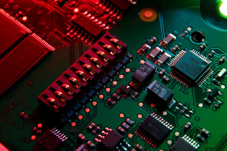
A major advancement in PCB assembly techniques was brought about by the introduction of surface mount technology (SMT) in the 1980s. Through-holes were no longer necessary for SMT components because they could be mounted directly onto the PCB surface, with the exception of a few specific applications. As a result of this breakthrough, PCBs and component sizes shrank, making it possible to produce electrical devices that were lighter, more energy-efficient, and more compact. By increasing the degree of automation in the assembly process, the switch to SMT also greatly increased production efficiency and speed.
Parallel to the developments in assembly methods, there was significant progress in PCB design software. Early design procedures involved hand-drawn schematics and physical mock-ups. Using computer-aided design (CAD) software changed everything by enabling the precise and error-free creation of complex designs. By combining mechanical and electrical design elements, modern PCB design tools allow designers to model a PCB’s performance virtually before moving on to the manufacturing phase. The development of complex electronics, such as those found in wearable technology, smartphones, and sophisticated automotive systems, has been greatly aided by this integration.
Automation has become increasingly important in PCB assembly; robotic systems are now used for everything from soldering and inspection to component placement. The quality and consistency of electronic products have improved along with production rates thanks to these advancements. Furthermore, even more advanced manufacturing techniques are being made possible by the incorporation of machine learning algorithms and artificial intelligence (AI) into PCB design processes. By evaluating data gathered during the assembly process, artificial intelligence (AI) can improve quality control procedures, forecast probable manufacturing problems, and optimize PCB layouts.
The creation of flexible and 3D-printed PCBs is one of the most recent advancements in PCB technology. Modern wearable technology and devices with unusual shapes require flexible printed circuit boards (PCBs), which are composed of materials that can bend and flex. In the meantime, advances in 3D printing technology are starting to be seen in PCB production. These advancements offer the possibility of quick prototyping as well as the ability to create PCBs with intricate, multi-layer designs that were previously impractical or impossible to produce through conventional means.
Environmental considerations and sustainability have become integral to the evolution of PCB design and assemblies, reflecting a growing awareness of the ecological impact of electronic manufacturing. An electronics design company, for instance, might prioritize the use of recyclable materials and the reduction of hazardous substances, like lead in solder, to minimize its environmental footprint. The shift towards more sustainable practices is also evident in efforts to decrease waste through the entire lifecycle of a PCB. For example, companies are adopting processes that allow for easier disassembly and recycling of components at the end of a product’s life.
The evolution of PCB design and assembly has been marked by relentless innovation, transitioning from manual processes to advanced automated and AI-enhanced methods. This journey, driven by electronics design organizations, continues to push the boundaries of technology, promising even greater efficiency, sophistication, and sustainability in electronics manufacturing for the future.